It’s been a hell of a summer with loads of work at my dull dayjob so that I’ve almost forgotten about everything including this very blog. However once the hell cooled down a little bit I found myself with a few spare days and my usual itch to tinker for a little bit with something. It happened I also needed another linux single-board computer to do some dull geeky stuff. Instead of ordering one from aliexpress once again I dived into the junk and found this little dead piece of hardware:
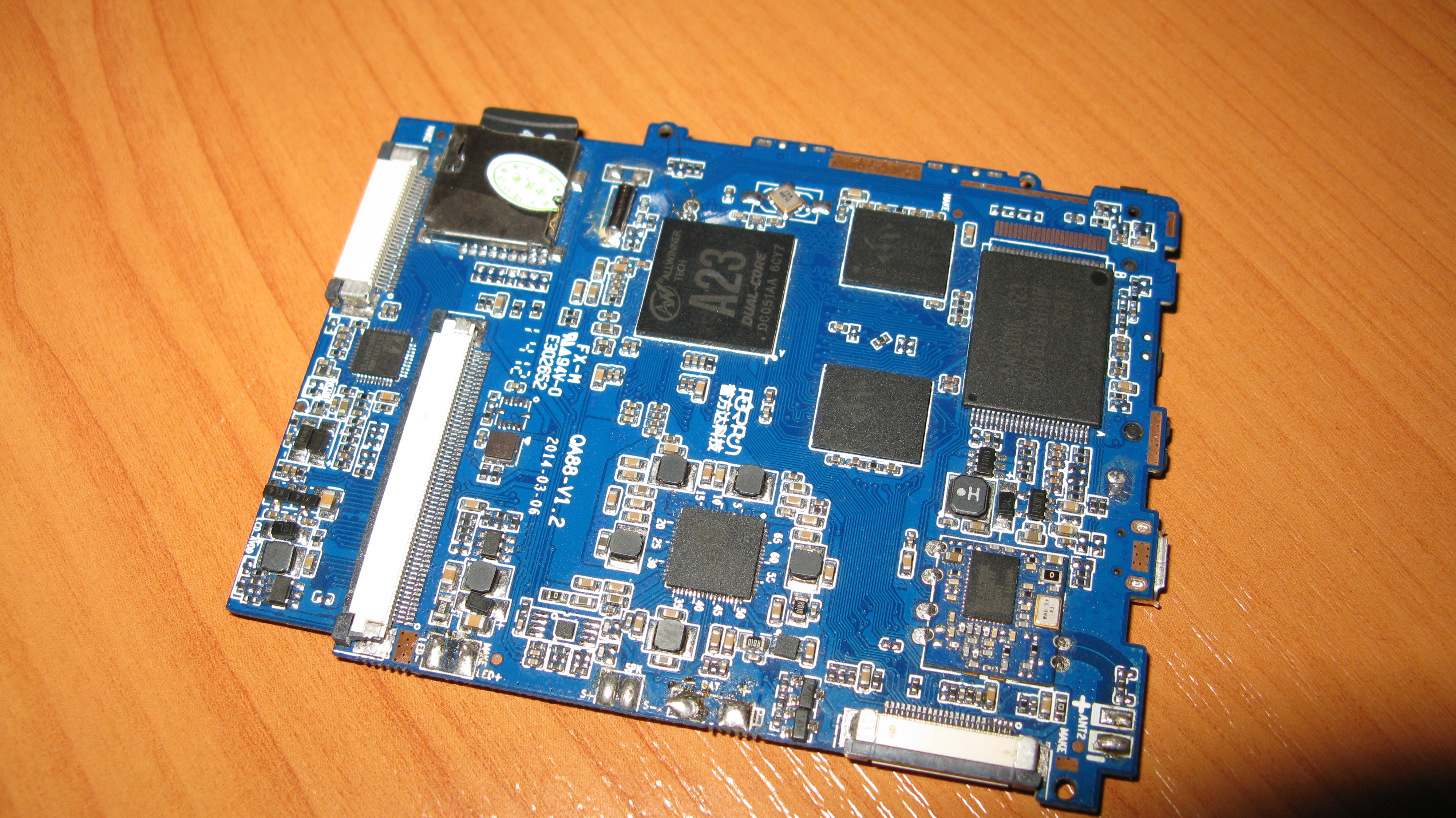
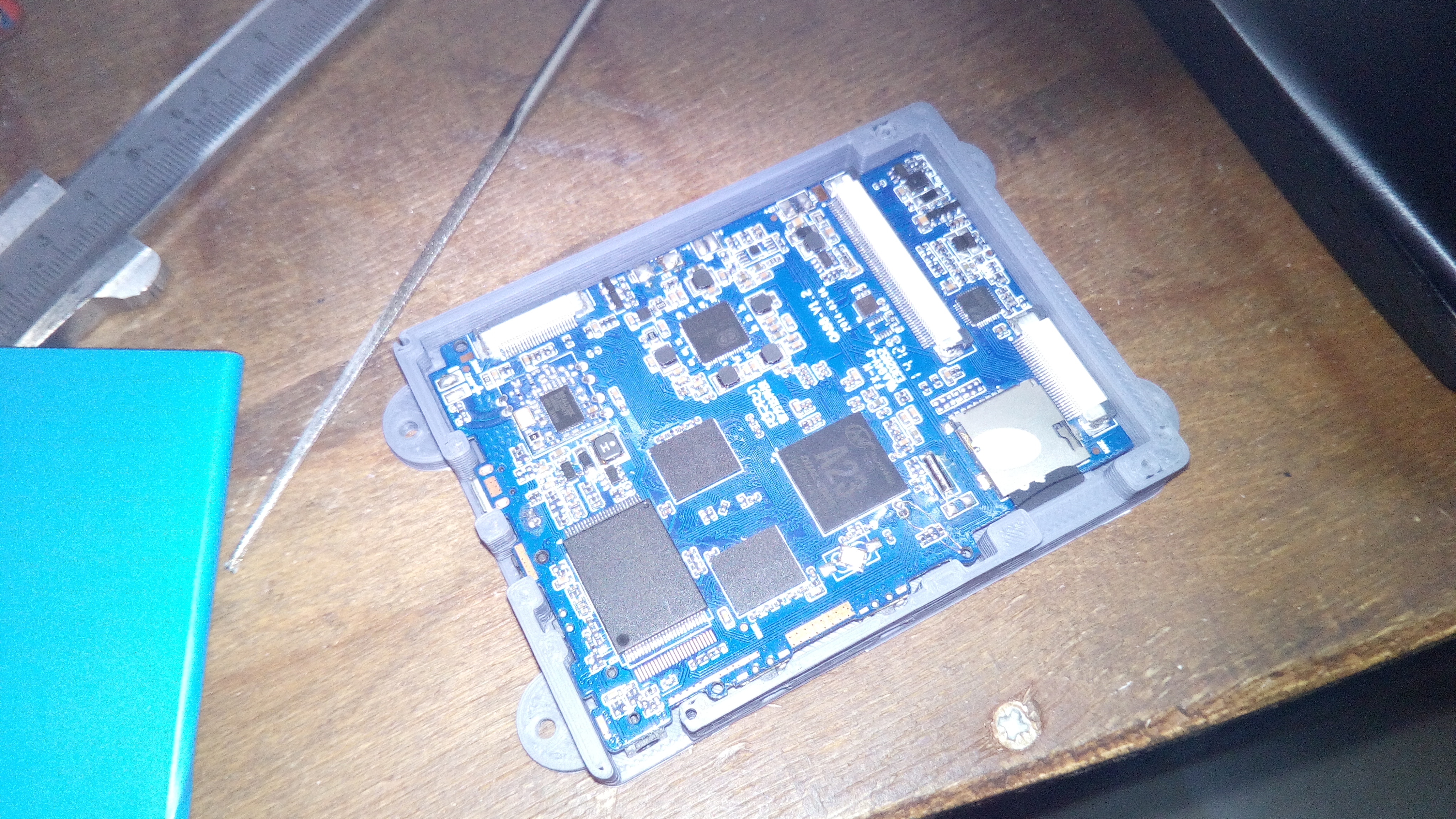
These are the guts of some cheap tablet PC based on Allwinner A23 SoC that died long ago. I got it from a friend when we decided to poke around A23 if it would be of any good for one of our projects (And we settled for Allwinner H3 in the end). Anyways this dead piece of hardware was sitting in my closet for over a year and I thought it was just about time to dust it off and make it into something useful. As it happened I also needed a small project to get familiar with Solvespace, a awesome free and opensource parametric 2d/3d CAD that was on my TODO list for learning for over a few months.
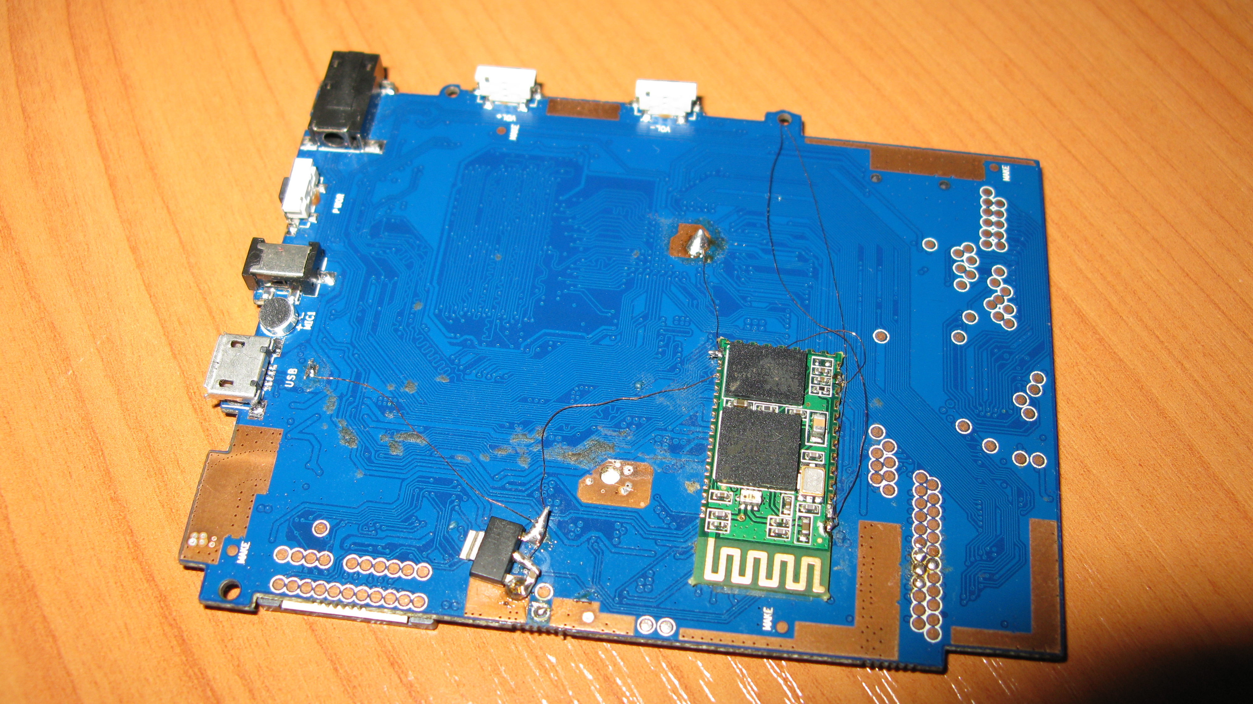
Okay, time to get things done. As usual I started by adding a HC-05 module to the serial port to the tablet and booted linux from an SD card.
This process is somewhat automatic for me, since I’ve done it for hell knows how many times. I started by compiling mainline u-boot and making a bootable SD card. Stock android that was still somewhere in NAND, but didn’t output anything on those UART pads. Nevertheless, once booted it provided me adb over usb with *SURPRISE* root access, so that I could pull the contents of the boot partition, including script.bin. That saved me the effort of brute forcing in search for relevant pads that get things done.
Once I got the serial terminal working I verified that I could boot mainline linux kernel and that everything works more or less reliably and the root filesystem created with skyforge works. This was the part when I put the code aside and fired up solvespace. The good thing about this CAD is that it’s:
- Simple as hell (took me less than 30 minutes to find my way around, an hour to start designing happily)
- It’s parametric!
- It’s easy to place a bunch of lines and later constrain them with the help of calipers to take form of a very complex shape. Precisely the thing that’s is very difficult to make with OpenSCAD
As you see in the picture above the PCB has a rather complex shape that took some time to constrain, even though I made a few simplifications. I ended up with something like that: 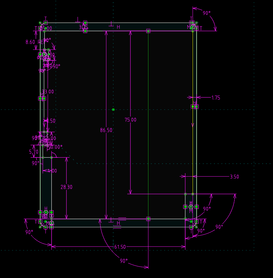
I added small ‘support’ regions so that the PCB would be always horizontal.

The basic approach for designing stuff like that is:
- Sketch the solid outer layer
- Extrude it for a few mm (green on the pic above)
- Start sketching on the surface of that brick, contrain the outer part on the lines below
- Extrude it all up.
- Sketch on different surfaces and extrude to add cuts for all the connectors
- …
- PROFIT
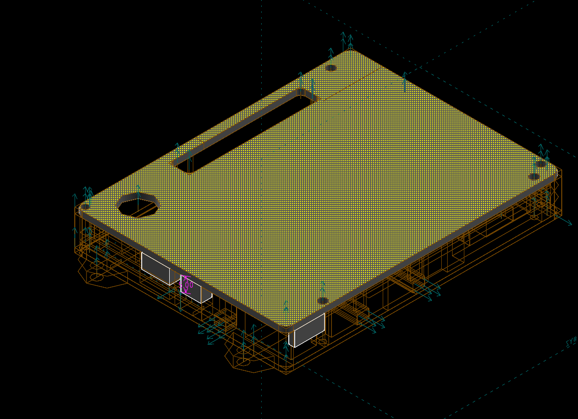
As you can see I’ve even added everything required for a nice wall mount. The next part of this enclosure is a separate compartment for:
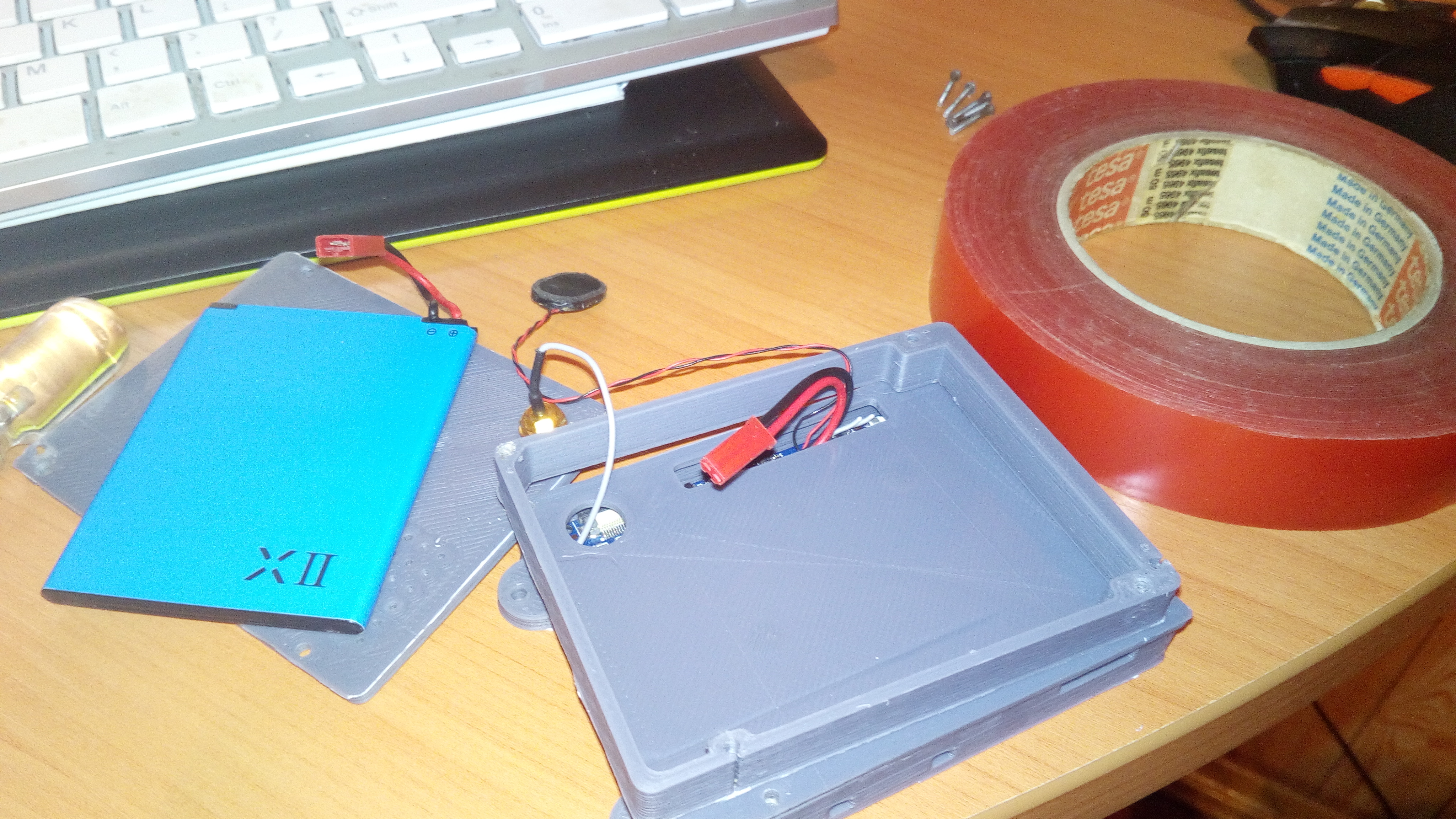
- 3.7v LiIon Battery (If we have a proper PMIC and battery pads, why not use them?)
- Speaker (Same as the above)
Bright 1-3W LED light (We have a step-up LED driver rigged to PWM of the SoC!)Turns out that part of the PCB was toast and I had to remove the LED.
In SolveSpace making a part that has to fit the one you’ve designed before is quite easy. In order to avoid copy-pasting you start a new project, press New Group -> Link/Assemble and it will import your previous file as one group, so that you can constrain against it. You can suppress that group’s solid mesh with the relevant tick in the floating menu, turning it into virtually a ghost.
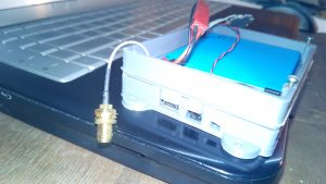
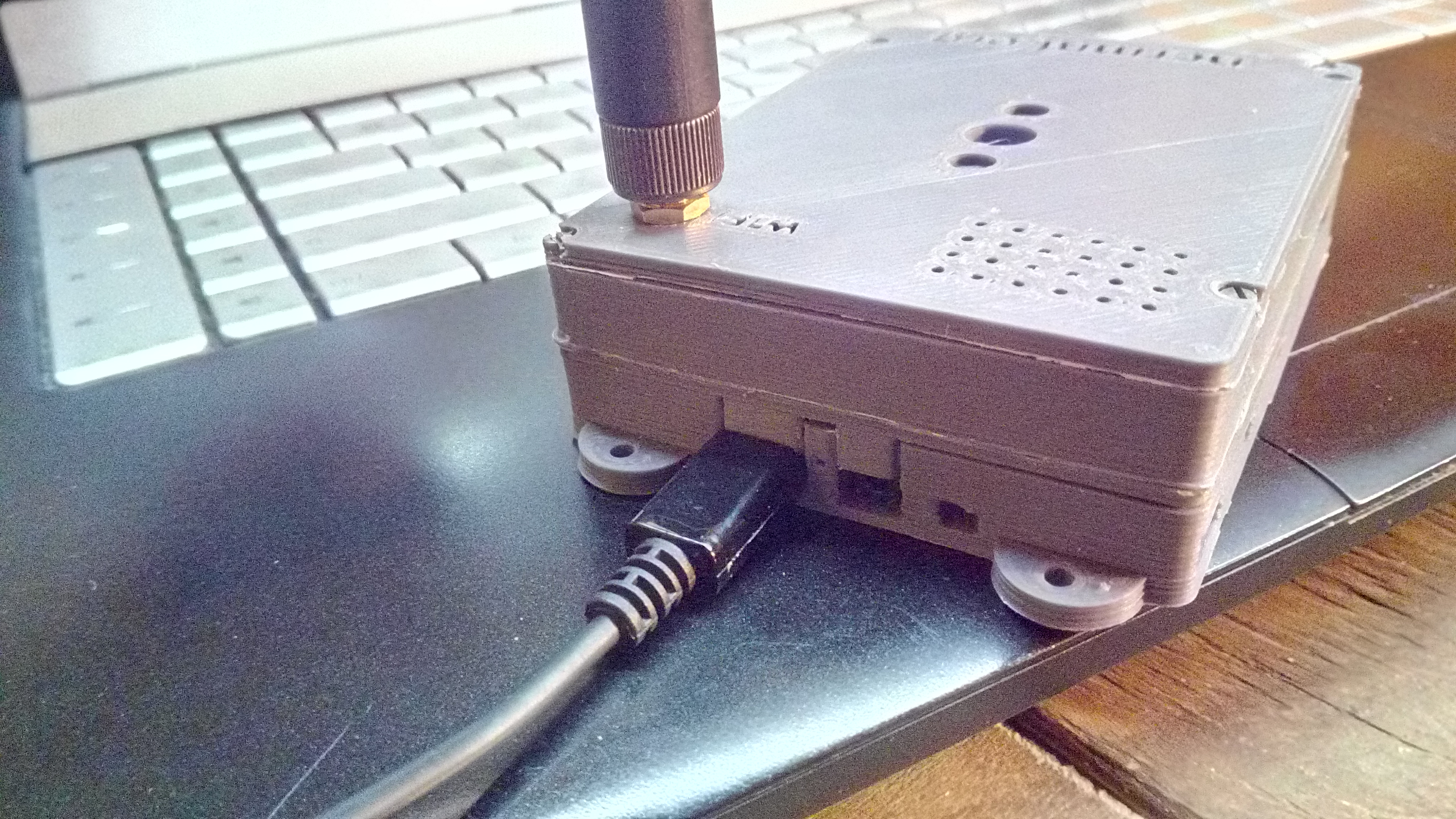
That’s how I’ve made the cover with holes for WiFi antenna cord and speaker/battery cables. Should I edit the bottom part, all the upper one will immediately catch up.
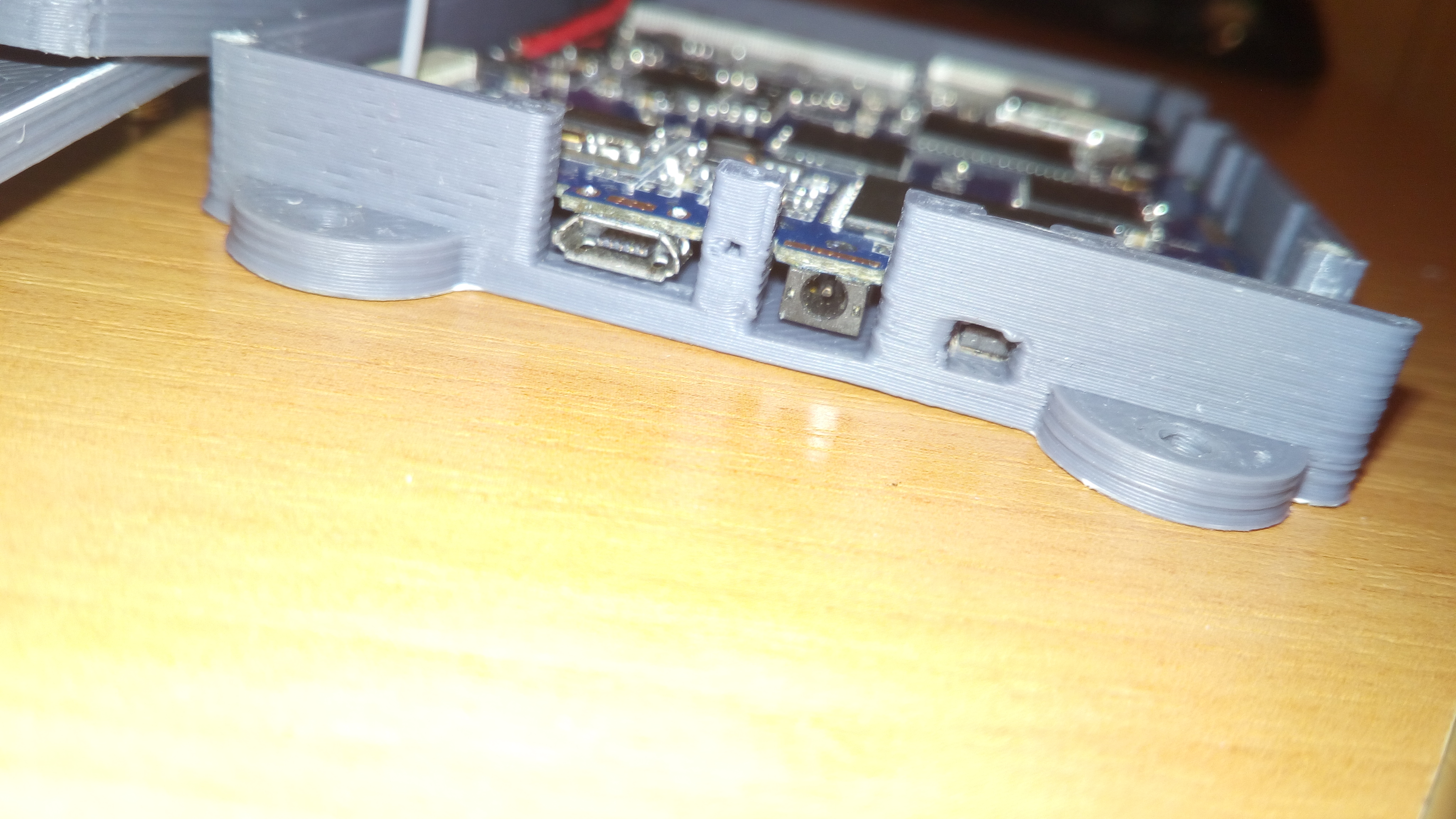
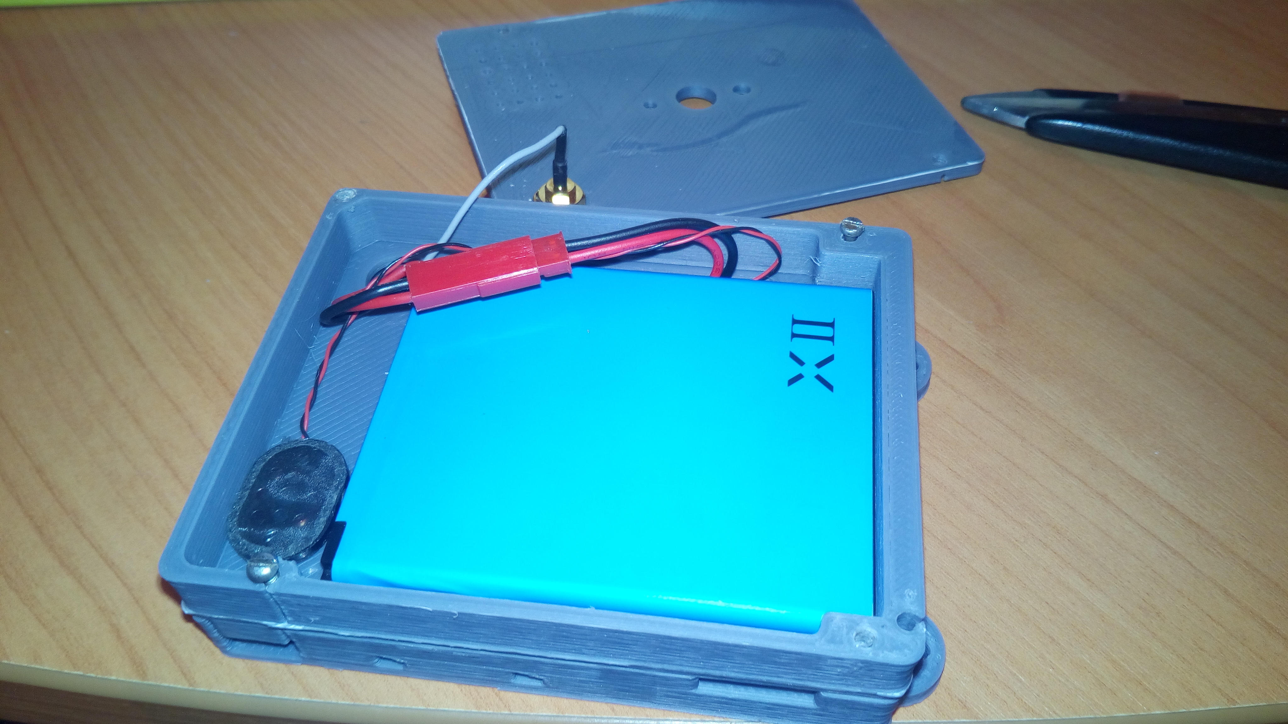
The pieces of plastic at the bottom tightly lock the PCB in place.
Next layer are basically the walls to house the battery and the speaker, nothing fancy.
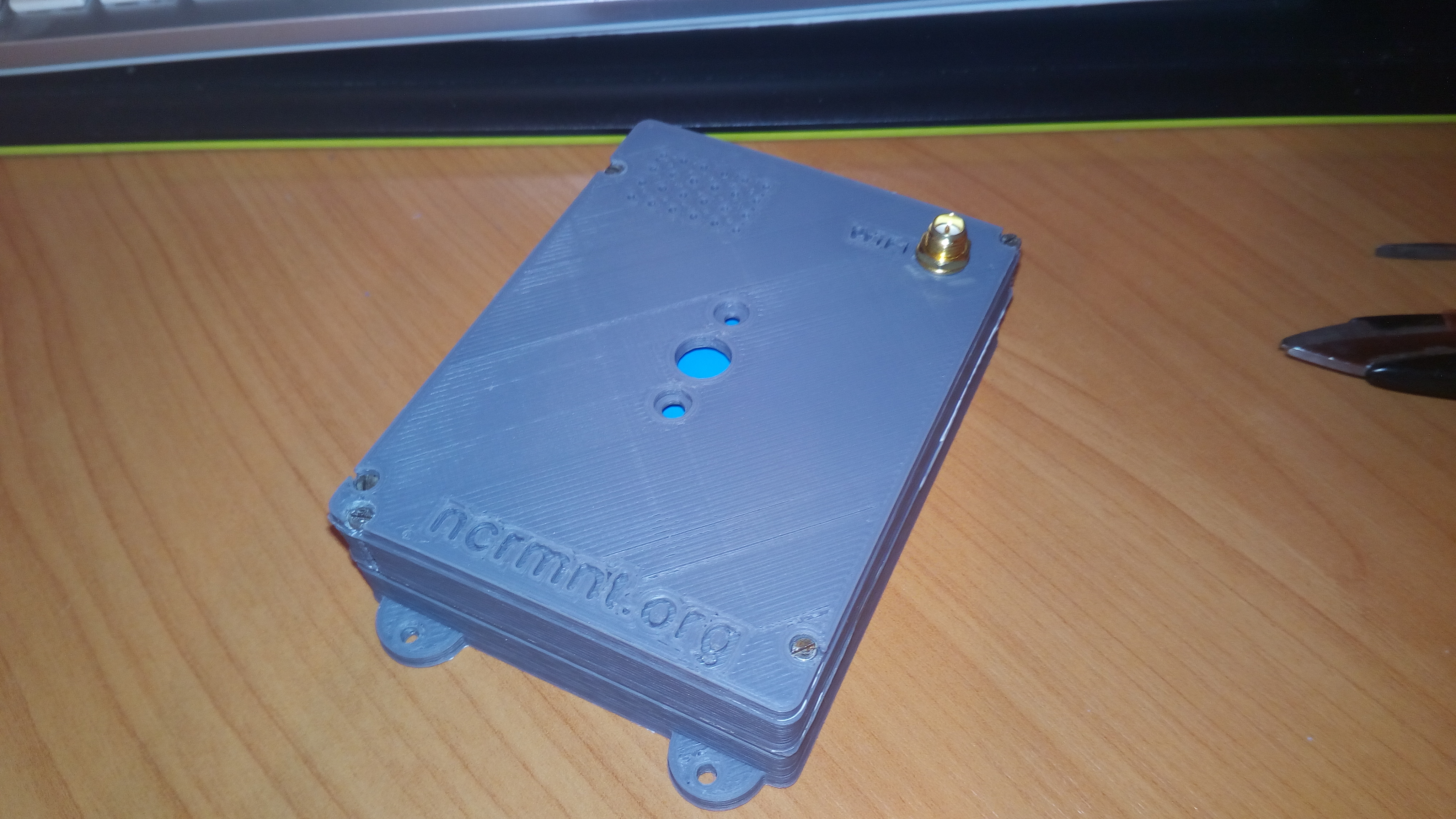
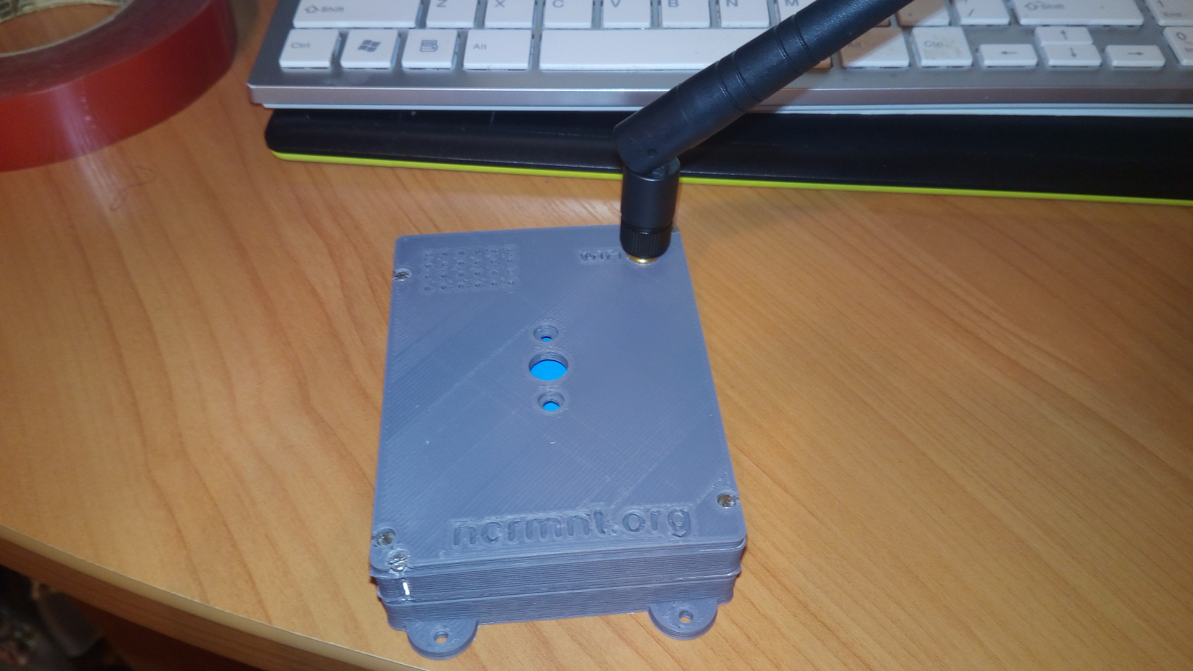
 The final part is the top cover. The top cover features a set of 2mm holes for the speaker to be heard, a hole for the SMA antenna pigtail and a few curved text labels to show off.
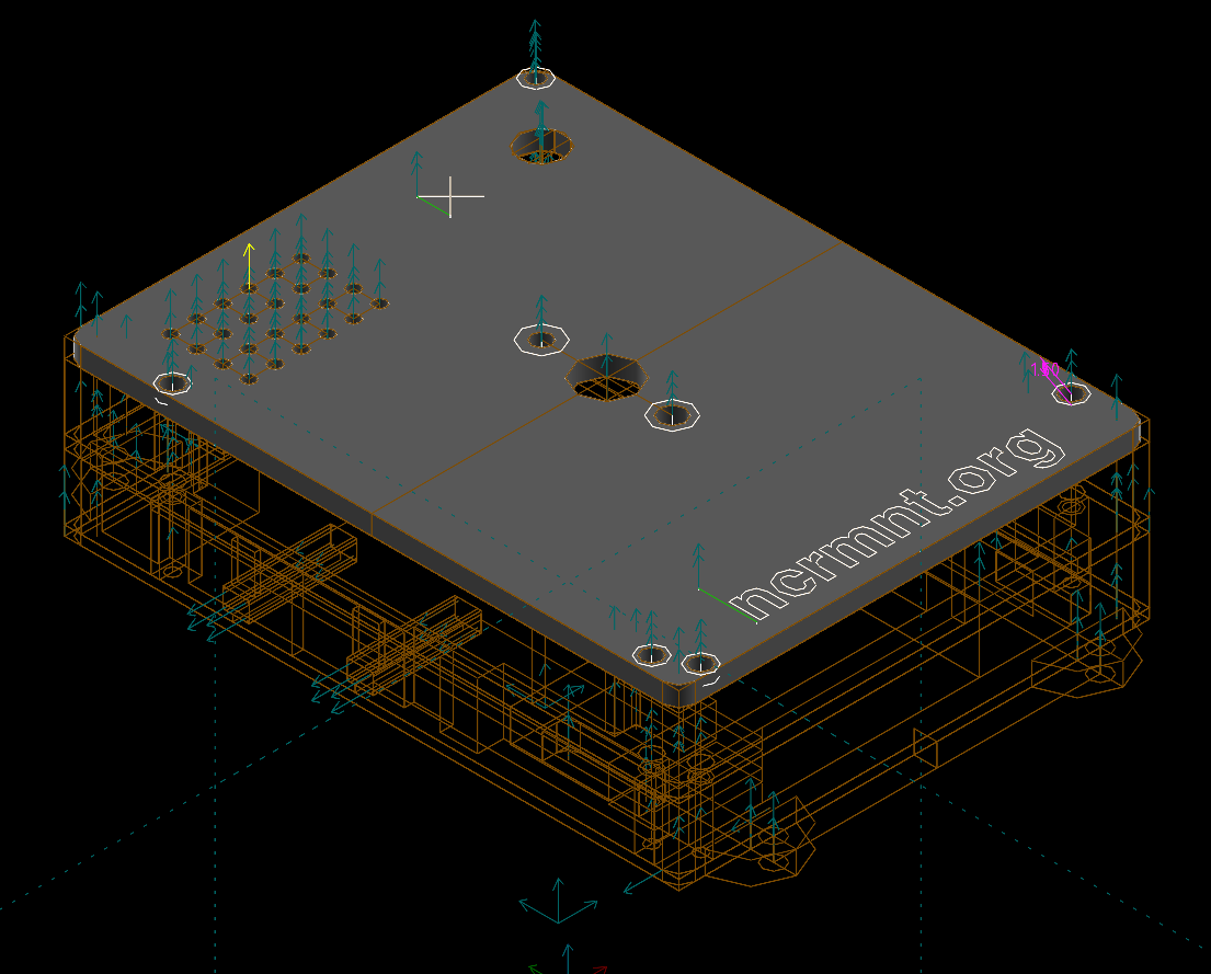
I also had a place for 1W LED there, but since the PWM circuit on the board was toast and the LED power was always on I had to ditch the LED for good. After all I found no way anyone actually would want to use it for.
Now, print time! It took me about 3 attempts to get the sizes right for the bottom layer so that the PCB would fit in nicely and without any stress that could ruin it in the long run.
 The next layers tightly locks the PCB in place. Battery and speaker are glued to it using the double sided sticky tape.
 And, finally, the top cover!
 …and the antenna
As a result of this hackery we get a battery backed SBC in a nice case that can be wall-mounted and has got some tasty specs:
- 1GB RAM
- Dual-core ARM Cortex-A7 @ 1.5Ghz
- 1 x USB OTG
- 8GB NAND
- 1 x SD card slot
- 1 x 3.5mm audio jack
- 1x speaker
- 1x 2500 mAh battery
- 1x microphone
- 3 buttons
- 1 x WiFi b/g/n
1 x High power LED driver with PWMThat one was toast!
Now, who is gonna say that raspberry is any better that this one? 😉
P.S. You can grab this design at thingiverse and print it.
Great job. Love the idea. I have a couple tablets that are messed up in one way or another. I might as well have a little fun with them.
You could also reconfigure those LCD connectors to use them as GPIOs. With the Fex format, it is quite easy to do. Then you need some flat ribbon cable to connect them to an adaptor in 2.54mm spacing to be able to use them properly.
Actually, LCD connector pins are all on the test pads. However I don’t want to use those. I prefer to connect all the homebrew stuff via USB. Yes, that’s sometimes a little overhead, but it makes things interchangeable, for I can’t rely that the next hardware brick I get will have the same number of GPIO pads.
Can U provide small step by step for building an SD card image for a23 tablet?